
Process Window Optimizer for pattern based defect prediction on 28nm Metal Layer
Résumé
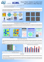
At the 28nm technology node and below, hot spot prediction and process window control across production wafers have become increasingly critical. We establish proof of concept for ASML's holistic lithography hot spot detection and defect monitoring flow, process window optimizer (PWO), for a 28nm metal layer process. We demonstrate prediction and verification of defect occurenceon wafer that arise from focus variations exceeding process window margins of device hotspots. We also estimate the improvement potential if design aware scanner control was applied.
Fichier principal
 20160210_Process Window Optimizer for pattern based defect prediction on 28nm Metal layer_POSTER.pdf (1.15 Mo)
Télécharger le fichier
20160108_ProcessWindowOptimizerForPatternBasedDefectPredictionOn28nmMetalLayer.pdf (1.25 Mo)
Télécharger le fichier
20160210_Process Window Optimizer for pattern based defect prediction on 28nm Metal layer_POSTER.pdf (1.15 Mo)
Télécharger le fichier
20160108_ProcessWindowOptimizerForPatternBasedDefectPredictionOn28nmMetalLayer.pdf (1.25 Mo)
Télécharger le fichier
Origine : Fichiers produits par l'(les) auteur(s)
Origine : Fichiers produits par l'(les) auteur(s)
Loading...